This page is devoted to the classic PC soundcard, Adlib, and compatibles.
Reverse-engineering report
2008-04-20
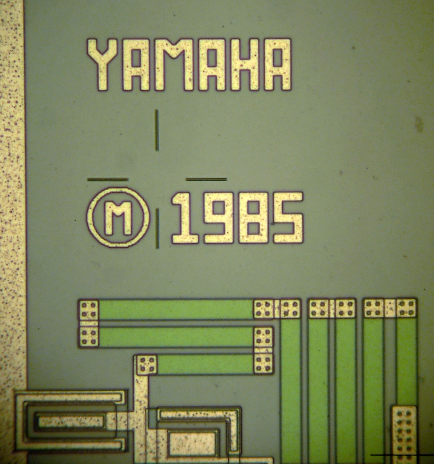
Me and Matthew Gambrell reverse-engineered the YM3812/YMF262 ROM tables. These are the pictures we took:


The bits of dirt are from my fingers, sorry about that.
See also: Yamaha YMF262 die images.
Exponential table functionality test
Here's an Excel file that shows how to use the exponential table.
Adlib-DigiSnap
2000-03-06
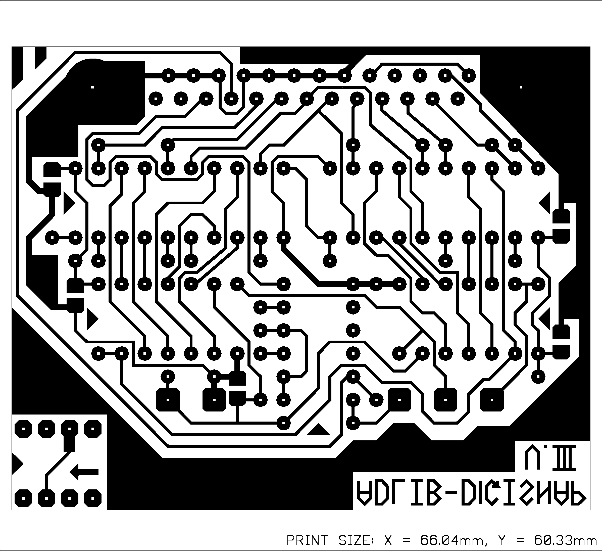
Adlib-DigiSnap (ads.pdf) is a device that is capable of recording Adlib (OPL2/YM3812) digitally. Want to build one? Now you can! You will also need the PCB film and the MSDOS driver (with source code, also a newer version 2009/01/11 with everything for compiling it is here).
Adlib Megamix № 1
Here (mp3) is a mashup of Adlib songs that I like, recorded using Adlib-Digisnap.
Hi Olli,
many thanks for posting your reverse-engineering results! I have long been trying to reproduce the sounds generated by YM3812 exactly. I tapped the connection between this chip and its DAC on an old Soundblaster and performed measurements with the help of an FPGA (which was configured to do essentially the same job as your DigiSnap). I wrote a program which controls the YM3812 at register level, or alternatively computes a string of sample values, which should exactly match the measured values. Only recently I discovered what you have achieved. Knowing the contents of the exp and log-sin tables, I finally can indeed replicate the sample values of at least the simpler sounds bit-by-bit. The whole stuff isn’t quite ready for putting it online, but if you are interested, I will of course share what I have. Again, many thanks!
Hellwig
Hi Hellwig! Sounds like a neat setup. I had something similar in mind, but after the microscopy work, I have not found the time to work on it anymore… So me and Matthew put the tables online for people like you. :)
rule!
Hi Olli. I have also verified on real YMF262 OPL3 chip that the tables and formulas in your reverse engineering report are accurate. I might add that the gain (or actually attennuation) is just a sum of Total Level (TL) register and ADSR Envelope Generator output. And since the gain also goes through the 256-entry table, gain has 8 fractional bits, so 0x100 means 6dB attennuation and 0x080 means 3dB attennuation etc. Total Level register has 6 bits and 48dB range, so 3 bits are integer part and 3 bits fractional. From OPL4 FM part datasheet it is shown that ADSR envelope has 96dB range and 0.1875 dB resolution (yes it is a typo in the datasheet), it means the envelope is a 9-bit value, 4 integer bits and 5 fractional bits. Sustain Level register bits also match the same gain formula when shifted into right position.
Thus, gain = (TotLev<<5) + (Envelope<<3);
Envelope is a linear ramp for decay and release, but attack is exponential curve and I have not been able to figure out the exact formula for it yet. The values may come from the logsin or exp table that are indexed linearly. Current emulators just approximate it, it would be nice to get it right.
I also found out the LFO table for tremolo effect, but it had been already figured out by Jarek Burczinsky in his YMF262 emulator, present in ScummVM, DosBox and MAME projects.
Some day, I could make an upgrade to your DigiSnap to use only two 74HC595 chips and an 74HC14 Schmitt trigger inverter instead of five chips it now has, and minor upgrade to software to leave out data conversion to record YMF262 PCM data too. I think OPL2 and OPL3 used different clock edges to load data out pin. For now, I use my USB logic analyzer.
Hello,
I’ve been looking for how to convert a value in the -logsin table to true values with only the exp table. I’va been using the data from the OPLx decapsulated.
The problem came from the ‘minus’ in the logsin. Thus it is not a logsin table but a log(1/sin) table.
The output format to the DAC must be noted : (from the datasheet of the YM3014B) (-1 + mantissa (with 2^^0, 2^^-1, 2^^-2 …)) * 2^^-exp bits.
So the data is in floating point format with 3 bits of exponent and 10 bits mantissa.
Whene you have the -logsin value you have the 8 LSB to look for in the exp table (I’ll explain how) and the other bits that are the exp of the FP output.
If LSB is not 0 you should convert it to a ‘positive’ value by taking 2^^8 complement (in fact it is as adding 1 to a negative number in [0..1[ range). It means that you are dividing by 2 the value (2^^(-x) = 2^^(1-x-1) = 2^^(1-x)/2)). Dividing by 2 is just adding 1 to the exponent (remember the 2^^minus in the YM3014B ?)
If LSB is 0, the mantissa is 0 and the exponent is taken as is from the MSB.
Off course don’t forget hidden 1 of the float format to have tha actual value.
I built one of these last night and it seems to work. But I’m using it to investigate the OPL3 chipset. This is interesting because it has 4 output channels rather than just 1 and each operator chain can be directed to any combination of output channels.
The data I collected last night was very noisy, but I’ve just been looking at the datasheets for the chip and it looks to me that the CLK signal is inverted in the OPL3 as compared to the OPL2. (The falling edge of LOAD corresponds with a rising edge of CLK) This would mean that I’m loading the shift register at the same time that the data is changing.
I built my device on a protoboard, so it’s easy for me to change. I’m going to use the last left over NAND gate to invert the clock and see if that fixes my problems.
I was mightily impressed by the microscope work as well. Many thanks to you, Olli
The clock signal is indeed the other way on the opl3. And using the last NAND gate sorts it out.
I should point out that Jani had already said that in comment #4, I just wasn’t paying attention.
Carbon14, IIRC, the clock edge is wrong regarding both data and load signals of OPL3. I never ran into any hardware problems with it though. I used about 2m of CAT5 cable so the signals were twisted with ground return.
Now the question is did you modify/rewrote the software so it records raw PCM, instead of doing conversion from the YM3014 format?
However I later bought an USB logic analyser so I don’t have to fiddle around with custom hardware or software, it just captures everything for later analysis while real-time analysis is not possible unless I write a plugin for that.
Jani,
I’ve been looking at Olli’s software today. I’ve been using the debugreader because I wasn’t certain that the OPL3 output was the same format as the YM3014 format. The YM3014 datasheet is explicit about it’s operation, but the YAC512 is much less so. Do you have details of the YAC512 format?
Formats between OPL2 and OPL3 are different. OPL3 uses straight 16-bit offset binary PCM – the format is described both in YMF262 and YAC512 datasheets, available by googling.
Value 0x8000 means silence 0, 0xFFFF means +32767 and 0x0000 means -32768. So to convert to signed 16-bit PCM what for example WAV format uses, just toggle the high bit with XOR if I recall correctly. As a guideline, a single operator outputting sine or square wave at full volume results in min/max amplitudes of +4084 and -4085 (yes there is a off-by-one artifact in the output because of the way the chip perhaps handles sign and magnitude internally, the negative sample values are just got by inverting the magnitude bits).
Sampling rate is 49716 when rounded to nearest integer in case you are unsure what sounds the best.
Long time no updates. I have been figuring out a few things.
In your decapsulation report you suggest the chip might accumulate the waveforms in floating point form. In the Yamaha Y8950 MSX Audio chip application manual, there is evidence how internal data from accumulator is converted to floating point, which gives evidence that in fact the accumulator works in PCM, which also gives evidence that operator output is PCM. It also makes sense for the operator output to be PCM, as it used as PCM in feedback path and in modulating the carrier phase. Plus all my calculations so far match on OPL3 (YMF262) in this way, and it only has PCM output, not floating point.
Also there was some talk about the frequency response of the output due to the analog filters and amplifiers. I was able to figure out that the DAC reconstruction filter has two Sallen-Key topology filters. In both filters, C1=C2=4.7nF and R1=R2=2.2kohms. Given the component values, both second order filters have cutoff frequency of 15392 Hz. The first filter has gain setting resistors of 12k and 10k, so the gain is 2.2, and the second filter has gain setting resistors of 1.5k and 10k, so the gain is 1.15. These gains very closely match design parameters of a fourth order Butterworth filter, which are 2.235 and 1.152 in my book. Still this does not take into account the whole system, like the floating point DAC, RC4136 op-amp, mute and volume stage with AC coupling capacitors, and the LM386 power amp, but would be a nice start to have matching digital filter on software chip emulator.
Jani: carbon14 has evidence that in OPL3/YMF262 the accumulator does not work in floating point: http://forums.submarine.org.uk/phpBB/viewtopic.php?f=9&t=1054
I believe the Google Doc has a typo – shouldn’t the MSB of the logsin output be used to index into the exponential table? Otherwise, the LSBs can overflow depending on the value and create a strange, Stegosaurus-backed sawtooth pattern.
I believe you want to essentially do this:
exponent[ (logsin[w] >> 4) ] + 2^-(logsin[w] & 15) or something along those lines if you’re talking about exporting out to a 13-bit floating point unit.
David, I think the doc is correct as it is. I’m attaching a spreadsheet demonstration to this page.
Thanks for the table, Olli! I think I understand what you meant with the exponential table better. I’m still confused out to use logsin[x] as input to exponential[x]. I’m not getting values I’d expect.
Say, for example, I want exp(logsin(50)). Is this correct? (exp[ logsin[50] % 256 ] + 1024) * 2^(logsin[50] / 256) ?
I’m trying to prove to myself that I can reconstruct a sine-like quarter waveform but I’m just not seeing it…
You need to negate the logsin output. If still no luck, add some large number to the already negated logsin output, for example 2048.
Excellent, I was wondering about that. Comment #5 was also of help. Thanks for your effort in bringing this information to us, Olli. I was really happy to find the tables and I appreciate the hard work that you guys put into this. I’m really pleased with the algorithm that this chip used, addition of log-transformed values is really a cool trick. Kiitos –
And by negation, most of the time with OPL chip it means inverting the bits (~X) instead of changing the sign (-X). Also if you are comparing to real OPL chip output, you have to double the value what you get out of the table. Yes I am also very grateful for this information, it helped me understand the chip more, but it seems almost everything I have reverse-engineered from the chip, they already seem to do it correctly in MAME emulator.
Cheers, David. :-) Yeah, it’s really good engineering that they did back in the day!
Hello. I’m not yet familiar with this subject, only built a phase accumulator that efficiently and reliably tunes accurately to LF and behaves as I want, in the last few days, but I aim to build an FM synth to test some ideas learned on an SY99.
While I have the log2(sin(X)) table, I haven’t understood the use of the pow(2,X) table to restore a sine value for output. As I’m not limited to the OPLn hardware for my schemes, I’m testing the maths in floating point for the pow(2,X) table just to see how it can work. I understand that pow(2,log2(sin(X))) will restore sin(X), but I imagine the point of the pow(2,X) table is to do this restoration with no multiplication, never mind maths functions, to get best speed.
Please can someone tell me how to do this in terms of floating point? Like David I’m getting initial results that make no sense to me, so I can’t figure out much from my errors. Once I can see it happen right in floating point I’ll have little trouble scaling it to integers to run fast like the stuff I already got working.
PS. Thanks for the detailed work, it (along with the short article here: http://code.google.com/p/music-synthesizer-for-android/wiki/Dx7Hardware) have been the most helpful data I found. For phase accumulators I fumbled my way as well as any I found, but for clues to optimising the methods for speed these pages have been extremely good.
Take a look at Carbon14 forum, you can find his webpage by clicking his name on his comment. We have this and many other discussions there. Anyway, the pow table is just indexed with 8 fractional bits, so the formula really is just pow(2,X/256) so X=0 means 2^0=1, X=256 means 2^1=2, X=512 means 2^2=4, etc.
Forgot to say, nice work with the DX7 reverse engineering. I have seen the schematics myself, and could only guess what the actual envelope and frequency (phase increment) buses transmit, but I had a pretty good guess nevertheless. I find it odd the phase increment is sort of logarithmic and is run through the exp table to get linear frequency increment. I wish I had a DX7, my friend did see one at a flea market, but another friend bought it when he found out. A rom dump would be nice to examine. I already figured out the address space used by the chips from the schematics.
Not mine. :) That DX7 bit I found… But it was my core starting point, along with posts various regarding phase mod versus frequency mod. I’m using different table sizes, not precise emulations of the OPL2 or 3 chip, I’m after better resolution than those, and my exponent table generator is different from the one described here and elsewhere. The basic idea is the same though, use lookup and addition throughout, for best speed. I don’t mind using bigger tables, they save interpolation, and reduce arithmetic in the inner loop, and still fit in a modest L2 cache. I’ll rethink all this if I ever decide to embed it in hardware, but I’m not that good right now.
Re DX7, get a TX7 on eBay. :) Same innards, a lot smaller, cheaper, easier to ship. Mostly, I’m listening extremely closely to the output of one of those and playing it by ear. The proof of the pudding, etc….
About that linear phase shift, I wondered about that too, I thought there ought to be a way to stay in log mode to avoid CPU cycles being wasted, but there seems to be a need to go back to linear there, regardless. The envelope generators sem to offer more interesting scope for invention, I found at least two ways to get them perfect, but so far only one that looks like being easy to convert to lookups and additions. I am NOT a mathematician, this comes painfully hard for me, but it is extremely interesting, and it has a knack of showing when it is correct, because it settles into a simple method whose results match exactly what my ears tell me about the original instrument. Can’t get a better ‘checksum’ than that.
SiliconPr0n seems to have classified the OPL3 (YMF-262) incorrectly as analog audio chip. I wish there was some easy way to give them feedback.
Hi Olli, I believe I have found out what the OPL2 third ROM with 16 entries of 7 bits is.
The bit patterns seem to match the Keyboard Scale Level feature, which attenuates higher notes more than lower notes. Just compare the ROM entries, or rather the difference between entries, to difference of this OPL3 table in Steffen Ohrendorf’s PeePeePlayer code : 0, 24, 32, 37, 40, 43, 45, 47, 48, 50, 51, 52, 53, 54, 55, 56. The index to the table is four high bits of the 10-bit FNUM value, and octave data is added later in the algorithm.
If I read the ROM bits correctly, the leftmost bit is LSB, unused and always 0. Some discrepancy may come from the fact that I am reading OPL2 die picture and the table values are verified with OPL3 chip. I noticed the ROM first non-zero entry has value 32 while based on code it should be 2*24=48, or then the values in ROM are again delta values from some offset that is not in the table.
Good detective work, Jani! It always bugged me what that table was.
Nice to see that someone found my code ;)
I have already fixed the code: http://sourceforge.net/p/peepeeplayer/code/ci/master/tree/src/ymf262/envelopegenerator.cpp#l31
And a big, big “thank you” for finding the formulas; without them, it wouldn’t have been possible for me to reach the goal of a bit-compatible emulator (anybody here who wants to contribute? ;) ).
Cheers!
Sto, I do contribute but on another forum ;) Maybe I should ask you commit access, but I am not so familiar poking around modular C++ code.
Fantastic work!
The Adlib Megamix is really nice also.
I recognized most songs, but do you have a track list? Especially the first song, it’s really great, and I never heard it before.
Never mind, found it, it is Grabbag from Duke Nukem 3D (the theme song). However, it sounds like it might be a different version than the regular one? Perhaps it is only the volume fade that makes it sound different.
Or, that it’s a mono Adlib version. From the MP3 tag, in no particular order: NHL94 Keen4+6 MK Wolf3d Duke3D Dune UFO Doom EOB2 SHOCK.EXE. MK is Mortal Kombat, EOB is Eye of the Beholder II, and SHOCK.EXE is a BBS ad, dunno where the music came from originally.
Jani, I think your formula for gain could be correct afaik, but there’s one minor flaw: with 0 gain(No attenuation and maximum volume envelope(which goes from 63 to 0, to sustain and finally back to 63 for silence) you’ll get the full sinus from the LogSin table as output. With maximum gain(Attenuation and volume envelope both being 63), the signal is enlarged to a way higher value.
So this would mean that the formula is correct, but gain is actually substracted(and clipping to 0) from the LogSin table lookup? This would make the LogSin start at 0, ramp up to Maximum (attack phase) with the specified volume and attenuation, ramp down to sustain level, hold the level, finally releasing to zero output when having finished the release phase? If not, gain would be adding the attenuation(which is actually amplifying instead of attenuating).
Hi Superfury. Well, sorry this comes a bit late (we have already discussed about this on Vogons endless times already havent’t we ;), but waveform value of 0 is max output, and you get max output when you index the exp table with 255, so you need to index the exp table in reverse. It’s because the values in the ROM table are positive, but they mean attenuation, or negative gain, because log of anything below 0 is negative which is canceled out by the multiply of -256 in the formula. So waveform value 1 means 1 step down (-1) from maximum so you need to index the exp table with 254.
Hello,
I am reverse engineering a YM2151 and writing an open-source implementation in verilog. I am half way through by now. I had actually used a full wave sine table (1024) samples for my ROM table. My values are also exact bit-to-bit with those of the real chip. After reading your work today I a going to try and reduce the ROM table to the first quarter of the sine only and see if I still get the same results.
Now, you say that you only saw two ROMs in the chip. In the YM21521 I am using a third large ROM, that contains the phase counter increments for each possible note in an octave. The user entered the octave, note and a note subdivision callled KF (key frequency) and the chip was able to calculate that phase increment. But for that, so far I am using a table (ROM). It looks to me like the YM3812 should also have a ROM for this purpose as the way it sets up the frequency is similar. Didn’t you see any other ROM?
You can visit some of the development I am doing in my website. As I am quite busy doing the actual reverse engineering and design work, the blog doesn’t have the latest developments.
And, of course, thanks for sharing this information. It really helps.
No the YM3812 has no note lookup table, the phase increment is set directly by the FNUM and scaled as per octave (BLOCK) and then with the operator multiple.
Most likely the lookup rom has entries for 12 notes and you get the FNUM, and if you want some frequency in between those notes then you use the KF as addition.
Hello. I’m working on a rendering (as opposed to exact emulation) of the 6 operator DX7.Please can anyone workign on the OPL3 emulation tell me if the detuning shows any of the oddities I’m about to describe?
Detuning at same depth beats at same rate in FIXED mode for same frequency as in RATIO mode. So far, so good, but detune in FIXED frequency mode causes faster beating at the low end of the keyboard, slower at the top end!
Also, there are some discontinuities likely due to quatisation at low resolutions that make it hard to model the precise action, specifically, low values for detune result in a collapse of detuning above some point on the key scale.
If that’s not weird enough, with larger values, detuning results in a DECREASE in beat frequency at the top end in ratio mode, likely related to whatever is going on in fixed mode.
Rather than try to guess any further, I’ll paste a data set based on duration from sync to cancellation of detuned carrier pairs, expressed as a fraction of the longest duration. (MNN means note number, ‘A’ in 9 octaves. Blanks are where detuning collapses and the carriers remain in sync.)
Detune MNN9 MNN21 MNN33 MNN45 MNN57 MNN69 MNN81 MNN93 MNN105
+7 0.0500 0.0250 0.0131 0.0078 0.0052 0.0035 0.0019 0.0020 0.0039
+6 0.0588 0.0294 0.0156 0.0104 0.0057 0.0039 0.0026 0.0026 0.0039
+5 0.0714 0.0357 0.0208 0.0114 0.0078 0.0052 0.0039 0.0026
+4 0.0909 0.0454 0.0278 0.0156 0.0104 0.0078 0.0052 0.0078
+3 0.1250 0.0624 0.0417 0.0208 0.0156 0.0104 0.0156 0.0078
+2 0.2499 0.1250 0.0625 0.0417 0.0208 0.0312 0.0156
+1 1.0000 0.5000 0.2501 0.1249 0.0625
-1 0.5000 0.2500 0.1250 0.0625 0.0313
-2 0.2000 0.1000 0.0500 0.0312 0.0156 0.0156 0.0078
-3 0.1250 0.0624 0.0357 0.0179 0.0125 0.0078 0.0078 0.0039
-4 0.0909 0.0454 0.0250 0.0156 0.0089 0.0062 0.0039 0.0039
-5 0.0666 0.0333 0.0192 0.0114 0.0078 0.0045 0.0031 0.0019
-6 0.0555 0.0278 0.0156 0.0096 0.0057 0.0039 0.0022 0.0019 0.0019
-7 0.0476 0.0238 0.0132 0.0078 0.0048 0.0031 0.0019 0.0016 0.0019
If anyone can help me make sense of this, please do. :) A lot of that looks very rational, but to render DX sounds well, I need a grip on the irrationality too.
Is there anyone here now?
I still haven’t figured out the DX7 detuning, but I do have some more clues:
Detuning halves-doubles with 1,2,4 coarse tuning integer values, and follows transposed key pitch as described in my previous post here. It also follows keys in fixed mode! It may use a note number based table. It could be easy (if inefficient) to populate a table of up to 128*14 elements, but it’s a nasty notion. If anyone reading this has worked with detuning on a DX7, please post if you can help with a better way.
In case people did not post in answer to my previous post on detuning, thinking perhaps that what I offered is nothing in exchange for my questions, or is irrelevant, please take advantage of my offer of a free DX7 editor at http://lostgallifreyan.net which, if I get the info I need to finish the job, will also become a very cheap (or maybe free) emulation of the original DX7. It’s not an exact emulation down to code and data details, but it is at least more accurate than the Native Instruments FM7. DX7 emulations have been done by others, but mine is a very independent method, it owes plenty to Yamaha expired patents, and to clues on pages here, and to service manuals, but nothing to Dexed and Hexter, which I never even managed to get running on my systems, nor could I fathom even part of their large source code base, being mainly why I built my own! It took a while, but it was easier starting from base principles than to wade through source code that looked harder to follow than it was to write my own!
Is anything known about how the Percussion instruments on the OPL2 works? So how are each of those signals generated(using the RNG)?
I’ve managed to get it running mostly, but percussion still sounds off(based on OPL3EMU atm)? Melodic channels working 100%.
https://bitbucket.org/superfury/unipcemu/src/a456dac9d6b0d39731e0de50579fe94a6ef43b5b/UniPCemu/hardware/adlib.c?at=master
Just to leave it here, eight years after the fact, re: the exponential table and using the least-significant bits (which wasn’t immediately intuitive for me, either). It’s as simple as:
2^a+b = 2^a * 2^b
And, if n an integer greater than one then:
2^n = 2 << (n – 1)
Better than that, if m and n are any old integers then:
m*2^n = m << n
For the exponential table you're starting with a fixed-point number that has eight bits of fractional content. So it's a+b where a is an integer and b is a fraction. Decompose that into 2^a * 2^b, use the lookup table for 2^b and then use a bit shift to multiply by 2^a.
Related to the problem, but as I did it for a 6-operator synthesizer:
EXP[X&4095]>>(X>>12)
Where EXP has 4096 elements, filled like this:
N=4096; while(N–)EXP[N]=pow(2,-N/4096.0)*524287.5;
Ignore the final multiplier unless like me you want to allow 24-bit audio outputs. Scaling to 32767.5 or less is more usual. Polarity is restored later in the business.
The bitshift for X is always the number of bits needed to define the size of the table, so it can be smaller, or larger. I wanted very good sound, but 2048 elements works well too. The input to the Exponential function is a logarithm of a cosine, scaled and clipped to fit a 16 bit word, but I later found a native 32 bit integer to be faster, and the lack of need for clipping allows deeper nulls in the output sound, so less of those small spurious signals that anyone familiar with the DX7 knows entirely too well…
This is a bit opaque to me, and I’m trying to figure out how I’d implement such a thing. I can write the Verilog, if I can understand what it’s actually doing.
When the operator’s output is exp(logsin(phase2 + exp(logsin(phase1) + gain1)) + gain2), what are these phase2, phase1, gain1, gain2? I see the LFO provides vibrato/AM into the phase generator and envelope generator, which are both fed into the operator. I guess phase generator is ‘phase’ and envelope is ‘gain’, so what I’m getting is to take from the exponent table and logsin table at the indexes corresponding to these figures.
Thing is I don’t see where two phases and two gains come in?
Anyone knows exactly how the OPL2/3’s gain is calculated? And with KSL and the like that applies to it? I simply took the opl3emu’s (or Dosbox’s, can’t remember) algorithm for that so far and want to create a clean implementation to remove that final piece of borrowed code from my project.
From what I can find, I can’t find any description on how that part of the gain works, other than the Output Level itself.
The exact speed of the envelopes (in integer samples), how the attenuation is accumulated on a real chip, sustain level, KSR, KSL, A/D/R rates?
Also, Jani, so far I’ve made it to work with the exponential table by indexing by reversing the whole input (all bits but the sign bit, so substracting it from 1FFFh), but do you literally mean just the lowest 8 bits? Just reverse the lowest 8-bits (255-x) and leave the exponent alone?
Managed to figure it out. You’re supposed to flip the 8 bits for the exponential table lookup. Then after adding the hidden bit (1024), multiply by 2 (at least for OPL3 (or OPL3 mode), probably not on OPL2 (mode). And finally, the exponent value is used to divide by the power of two, not multiply.
Various songs I tried sound a lot better now! :D
Is there any difference between OPL2 and OPL3’s exponential table lookup outputs? Should the exponential table lookup including hidden bit always be multiplied by 2 for both YM3812 and OPL3 chips?